PVD-PECVD

Trusted expertise in vacuum coating technologies
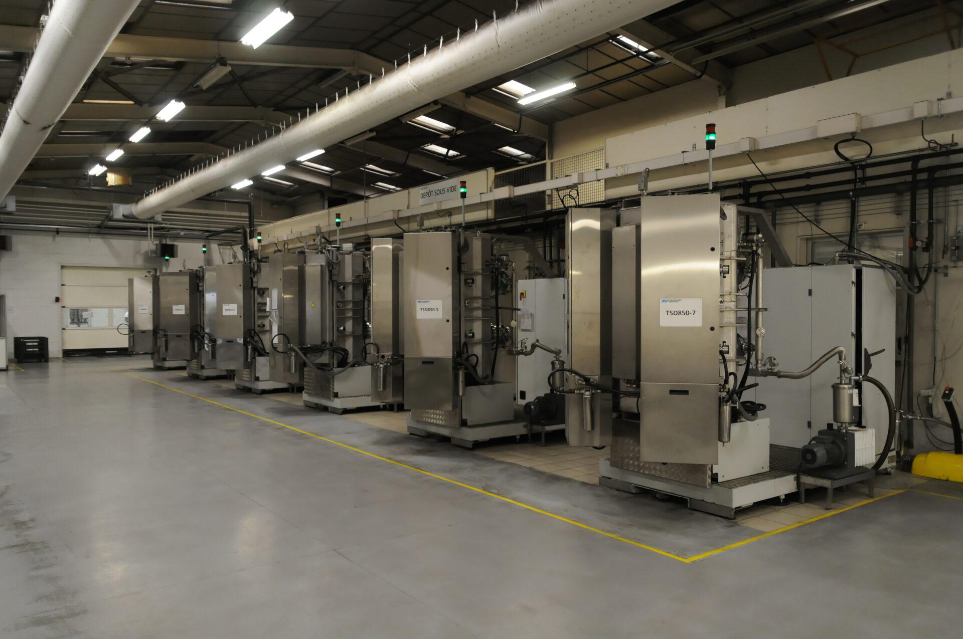
For over 30 years, IREIS has been developing and refining vacuum deposition technologies, in particular magnetron sputtering (PVD) and plasma-assisted chemical vapor deposition (PACVD). This research covers the entire value chain: materials development, process control, equipment design, right through to industrialization. Thanks to this integrated approach, IREIS is able to offer solutions tailored to the most complex needs, in a wide variety of industrial sectors.
Versatile technologies for all types of substrates
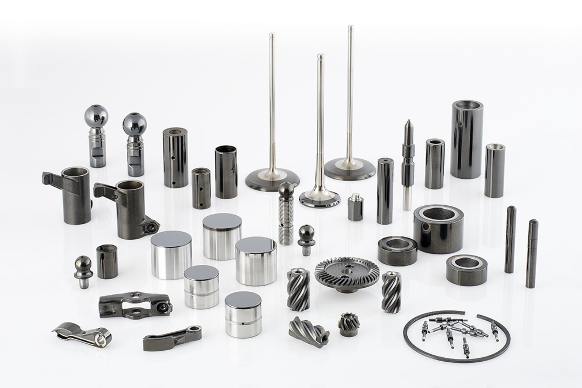
PVD and PACVD processes can be used to deposit a wide range of materials — metals, ceramics, nitrides, carbides, DLC, etc. — on various substrates (metals, polymers, ceramics, composites, etc.), subject to their vacuum compatibility. These thin films, with thicknesses ranging from a few nanometers to several tens of microns, enhance surface properties such as wear resistance, corrosion and erosion protection, as well as tribological, optical, or electrical performance. IREIS has both standard and specialized equipment to process complex parts and non-standard formats.

Proprietary processes for customized performance
IREIS has developed several proprietary vacuum deposition technologies: PEMS™, for dense, hard, low-friction coatings; CAM™, for very low-temperature deposits with excellent tribological behavior; and M-ARC™, which reduces defects in arc-evaporation coatings. These technologies enable IREIS to offer a comprehensive range of coatings under the Certess™ brand (CARBON, NITRO, OPTAL, LOOK, EJECT, LIFE, ELEC), each designed to meet specific industrial requirements.
An integrated organization and a global presence
The group’s vertically integrated model — encompassing research, equipment manufacturing, and consumables production — ensures responsiveness, competitiveness, and complete quality control. With over 70 years of experience in tribology and surface engineering, IREIS supports industrial clients worldwide with tailor-made solutions that meet the highest standards and offers production capacity suited to large volumes.